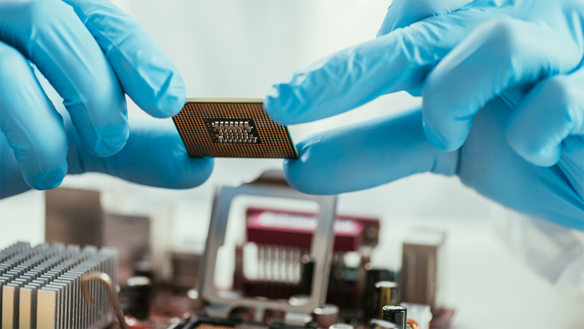
The technology sector is one of the world’s fastest-moving and most innovative industries, continuously pushing the boundaries of miniaturization and performance. Precision chemical machining (PCM) is helping to drive innovation in microelectronic design, with the innovative process delivering a level of precision, design flexibility, and cost-effectiveness that traditional machining methods can’t match.
Photofabrication Engineering, Inc. (PEI) is a leader in precision chemical machining, serving industries that demand micro-scale accuracy and repeatability. Standing shoulder to shoulder with our technology partners, we consistently deliver precision metal parts and components used by industry-leading computer, communications, and microelectronics manufacturers.
This article explores the importance of PCM in microelectronics and how PEI’s expertise ensures manufacturers receive high-quality, repeatable, and cost-effective solutions for their microelectronic design needs.
Why Precision Chemical Machining is Critical for Microelectronic Applications
As electronic devices continue to shrink in size while increasing in complexity, the demand for ultra-precise, high-quality components has never been greater.
Precision chemical machining, also known as chemical etching, is a fast, precise, and cost-effective manufacturing process that makes it ideal for microelectronic components.
Here’s why:
High Precision & Complexity
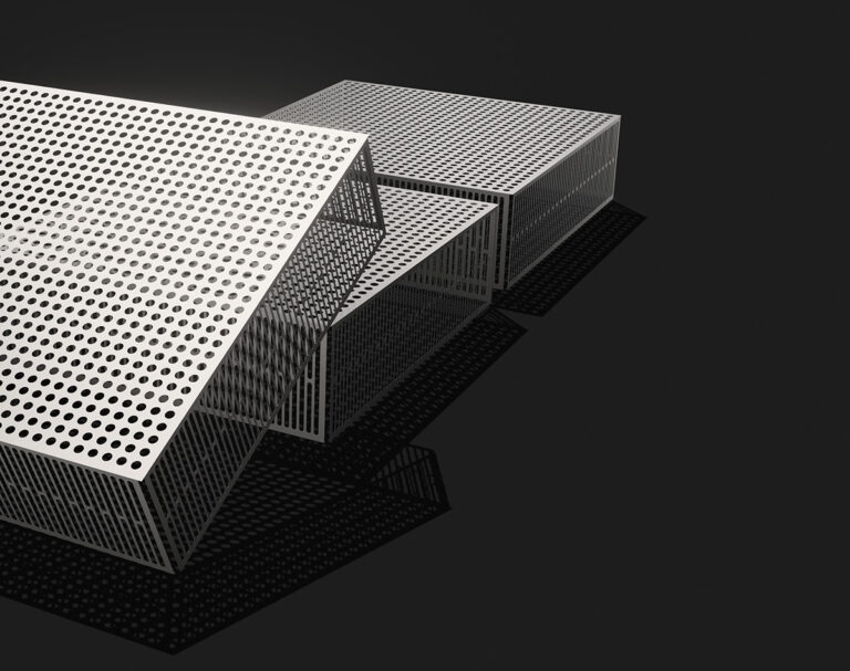
PCM can produce extremely fine features with tight dimensional tolerances, making it ideal for intricate microelectronic components. The process allows manufacturers to create ultra-thin, highly complex metal parts that other methods cannot achieve.
Material Integrity
Unlike mechanical or thermal processes such as laser cutting and stamping, PCM does not introduce mechanical stress, thermal distortion, or burrs. This ensures that microelectronic components maintain their integrity, which is crucial for high-performance applications.
Cost-Effectiveness for High-Volume Production
PCM is a highly scalable process. It allows for rapid prototyping and a seamless transition to high-volume production without expensive tooling costs. Manufacturers can quickly iterate designs and bring solutions to market faster.
Miniaturization Trends
With the push for smaller, more efficient electronics, PCM enables the production of intricate, lightweight, and high-performance components.
The PCM process consists of several important steps. Each step is a critical prerequisite to the next. PEI leverages the latest technology and tried and true processes to produce precise, thin metal parts, depending on the size, volume, complexity, and level of definition required for each new part.
Dry Etching vs Wet Etching
Wet etching and dry etching are crucial techniques applied in semiconductor manufacturing.
Wet etching involves chemical solutions to remove material and is effective for isotropic etching, where the etch rate is uniform in all directions. It’s a simple and cost-effective technique, but it lacks the precision required for intricate patterns and can lead to undercutting. When applied to a silicon wafer, this process often requires a masking layer to protect specific areas from being etched.
Dry etching, which includes methods such as plasma etching, reactive ion etching, and ion beam etching, uses gasses and plasma to etch materials. Dry etching allows for anisotropic etching, providing precise, directional etching critical for creating detailed semiconductor devices. While the dry etching process offers superior control and accuracy, they are generally more complex and expensive than wet etching, especially when you look at plasma etching processes.
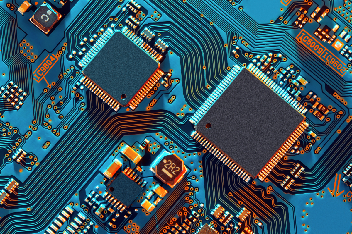
Key Applications of PCM in Microelectronics
Due to the precision and reliability produced by PCM, this innovative process has become a process trusted by leaders in microelectronic design.
Some of the most significant applications include:
Semiconductor Lead Frames
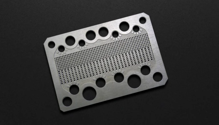
Thin, precisely etched lead frames are essential for microchips, ensuring optimal electrical connections and mechanical support for semiconductor devices.
Leading microelectronics manufacturers call on the team at PEI to produce surface-mount and insert-mount photochemically etched lead frames to meet exacting electrical, thermal conductivity, and strength requirements for companies providing integrated circuits. Engineers use these lead frames in semiconductors, glass-to-metal seals, and relays.
Our lead frames range in thickness from 0.5 mils [0.0127 mm] to 40 mils [1.575 mm], with features as small as 4 mils [0.10 mm] on 0.010 in. [0.254 mm) centers, creating lead frames that are strong enough to be handled yet flexible enough to allow bending when necessary. Learn more about our lead frames.
EMI/RFI Shielding Components
Electromagnetic interference (EMI) and radio-frequency interference (RFI) shielding are critical for protecting sensitive electronic circuits. PCM produces high-precision shielding components with custom designs to meet industry standards.
Our EMI and RF shield cans feature a patented, easy-access removable cover, enabling quick and easy repairs without damaging the surrounding shield. Learn more about our shield cans.
Microscale Interconnects & Contact Springs
PCM is critical for the production of flexible, ultra-precise connectors that facilitate reliable electrical connections in compact electronic devices. The innovative process enables the production of these microscale interconnects with high precision and repeatability.
Precision Apertures & Optical Encoders
PCM is used to manufacture highly accurate apertures and encoders for imaging and optical systems, ensuring superior performance in sensors, cameras, and other optical devices.
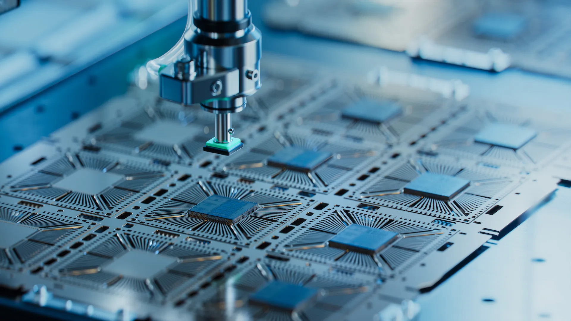
MEMS (Micro-Electro-Mechanical Systems) Parts
PCM plays a crucial role in MEMS production, delivering finely detailed etched structures for micro-scale sensors and actuators used in various high-tech applications.
PEI’s 55-year history includes innovations in microelectronics, delivering custom and standard metal parts such as lead frames, Kovar and molybdenum tabs, and chip carriers. We can etch virtually any metal, from basics like copper, brass, and stainless steel to precious metals (including silver) to exotic materials such as titanium, molybdenum, and beryllium copper.
Advantages of Precision Chemical Machining Over Traditional Machining Methods
When you compare PCM to traditional machining methods such as CNC milling, stamping, and laser cutting, a number of advantages put it clearly on top.
While conventional techniques have their place in manufacturing, chemical machining is superior in certain applications, particularly when dealing with delicate, intricate, or high-precision components.
The key advantages of PCM over traditional methods include:
Cost-Effective
PCM eliminates the need for expensive tooling and setup costs, making it a highly economical solution for both prototyping and large-scale production.
Tight Tolerances
PCM eliminates the need for expensive tooling and setup costs, making it a highly economical solution for both prototyping and large-scale production.
Intricate Geometries
PCM can produce highly complex designs that are not feasible with conventional machining methods, enabling greater innovation in microelectronic design.
Fast Turnarounds
With no tooling requirements and the ability to produce multiple parts simultaneously, PCM significantly reduces lead times, accelerating product development cycles.
Burr-Free Fabrication
Unlike mechanical cutting processes, PCM reduces surface roughness and does not produce burrs or sharp edges, ensuring that components meet the highest quality standards without requiring additional finishing processes.
Burr-Free Fabrication
Unlike mechanical cutting processes, PCM reduces surface roughness and does not produce burrs or sharp edges, ensuring that components meet the highest quality standards without requiring additional finishing processes.
PEI’s Expertise in Precision Chemical Machining for Microelectronics
With decades of experience in microelectronics manufacturing, PEI has become a recognized leader in precision chemical machining providing high-performance etched components used in semiconductors, sensors, interconnects, shielding, and telecommunications.
Our legacy of precision, dependability, and on-time delivery is essential when serving the technology sector and semiconductor industry, especially as the demand for faster, safer, and more reliable solutions.
Our precision photochemical etching process allows us to produce parts from 0.0005 in. (0.0127mm) to 0.1250 in. (3.175mm) thick, meeting the stringent demands of the technology sector.
We’re one of the few photochemical machining companies that can etch beryllium copper. Renowned for its exceptional hardness, strength, and thermal and electrical conductivity, this metal requires extra care because of the serious health hazards posed by beryllia dust.
We specialize in high-volume production runs, ensuring consistent quality and repeatability.
The Precision Microelectronics Parts We Produce
- Electrical Contacts
- Communications Components
- RF/EMI Shields
- Fan Screens
- Microwave Circuits
- Step Lids
- Flat Lids
- Gaskets
- Face Plates
- Screens
Redefining Etching in Microelectronic Design
Precision chemical machining is changing the game in microelectronic design, enabling the production of ultra-thin, highly complex, and precisely detailed metal components that power some of the technology sector’s most innovative devices.
With the advancement of miniaturization and performance, technology partners will need the confidence to know they’re working with a manufacturer specializing in precision PCM and providing fast turnaround times, high precision, and cost efficiency.
PEI is the world leader in precision chemical machining, delivering precise, durable, and reliable quality parts you won’t find anywhere else. Our precision chemical machining expertise comes from decades of experience and a daily dedication to perfection.
We boast a 55-year history of innovation in microelectronics, delivering precision metal parts and components used by industry-leading computer, communications, and microelectronics manufacturers. With our commitment to innovation and excellence, we continue to be a trusted provider of precision chemical machining solutions that are helping to shape the future of microelectronics.
If you need a proven PCM solution, the engineers, manufacturers, and quality assurance professionals at PEI are ready to answer any challenge. Contact us today or request a quote.